-
 Agriculture
-
 Health-Care
-
 Environment
-
 Construction-Real-Estate
-
 Tools-Hardware
-
 Home-Garden
-
 Furniture
-
 Luggage-Bags-Cases
-
 Medical-devices-Supplies
-
 Gifts-Crafts
-
 Sports-Entertainment
-
 Food-Beverage
-
 Vehicles-Transportation
-
 Power-Transmission
-
 Material-Handling
-
 Renewable-Energy
-
 Safety
-
 Testing-Instrument-Equipment
-
 Construction-Building-Machinery
-
 Pet-Supplies
-
 Personal-Care-Household-Cleaning
-
 Vehicle-Accessories-Electronics-Tools
-
 School-Office-Supplies
-
 Packaging-Printing
-
 Mother-Kids-Toys
-
 Business-Services
-
 Commercial-Equipment-Machinery
-
 Apparel-Accessories
-
 Security
-
 Shoes-Accessories
-
 Vehicle-Parts-Accessories
-
 Jewelry-Eyewear-Watches-Accessories
-
 Lights-Lighting
-
 Fabric-Textile-Raw-Material
-
 Fabrication-Services
-
 Industrial-Machinery
-
 Consumer-Electronics
-
 Electrical-Equipment-Supplies
-
 Electronic-Components-Accessories-Telecommunications
-
 Home-Appliances
-
 Beauty
-
 Chemicals
-
 Rubber-Plastics
-
 Metals-Alloys
- Masonry Materials
- Curtain Walls & Accessories
- Earthwork Products
- Fireproofing Materials
- Heat Insulation Materials
- Plastic Building Materials
- Building Boards
- Soundproofing Materials
- Timber
- Waterproofing Materials
- Balustrades & Handrails
- Bathroom & Kitchen
- Flooring & Accessories
- Tiles & Accessories
- Door, Window & Accessories
- Fireplaces & Stoves
- Floor Heating Systems & Parts
- Stairs & Stair Parts
- Ceilings
- Elevators & Escalators
- Stone
- Countertops, Vanity Tops & Table Tops
- Mosaics
- Metal Building Materials
- Multifunctional Materials
- Ladders & Scaffoldings
- Mouldings
- Corner Guards
- Decorative Films
- Formwork
- Building & Industrial Glass
- Other Construction & Real Estate
- Wallpapers/Wall panels
- HVAC System & Parts
- Outdoor Facilities
- Prefabricated Buildings
- Festive & Party Supplies
- Bathroom Products
- Household Sundries
- Rain Gear
- Garden Supplies
- Household Cleaning Tools & Accessories
- Lighters & Smoking Accessories
- Home Storage & Organization
- Household Scales
- Smart Home Improvement
- Home Textiles
- Kitchenware
- Drinkware & Accessories
- Dinnerware, Coffee & Wine
- Home Decor
- Golf
- Fitness & Body Building
- Amusement Park Facilities
- Billiards, Board Game,Coin Operated Games
- Musical Instruments
- Outdoor Affordable Luxury Sports
- Camping & Hiking
- Fishing
- Sports Safety&Rehabilitation
- Ball Sports Equipments
- Water Sports
- Winter Sports
- Luxury Travel Equipments
- Sports Shoes, Bags & Accessories
- Cycling
- Other Sports & Entertainment Products
- Artificial Grass&Sports Flooring&Sports Court Equipment
- Scooters
- Food Ingredients
- Honey & Honey Products
- Snacks
- Nuts & Kernels
- Seafood
- Plant & Animal Oil
- Beverages
- Fruit & Vegetable Products
- Frog & Escargot
- Bean Products
- Egg Products
- Dairy Products
- Seasonings & Condiments
- Canned Food
- Instant Food
- Baked Goods
- Other Food & Beverage
- Meat & Poultry
- Confectionery
- Grain Products
- Feminie Care
- Hair Care & Styling
- Body Care
- Hands & Feet Care
- Hygiene Products
- Men's Grooming
- Laundry Cleaning Supplies
- Travel Size & Gift Sets
- Room Deodorizers
- Other Personal Care Products
- Pest Control Products
- Special Household Cleaning
- Floor Cleaning
- Kitchen & Bathroom Cleaning
- Oral Care
- Bath Supplies
- Yellow Pages
- Correction Supplies
- Office Binding Supplies
- Office Cutting Supplies
- Board Erasers
- Office Adhesives & Tapes
- Education Supplies
- Pencil Cases & Bags
- Notebooks & Writing Pads
- File Folder Accessories
- Calendars
- Writing Accessories
- Commercial Office Supplies
- Pencil Sharpeners
- Pens
- Letter Pad/Paper
- Paper Envelopes
- Desk Organizers
- Pencils
- Markers & Highlighters
- Filing Products
- Art Supplies
- Easels
- Badge Holder & Accessories
- Office Paper
- Printer Supplies
- Book Covers
- Other Office & School Supplies
- Stationery Set
- Boards
- Clipboards
- Stamps
- Drafting Supplies
- Stencils
- Electronic Dictionary
- Books
- Map
- Magazines
- Calculators
- Baby & Toddler Toys
- Educational Toys
- Classic Toys
- Dress Up & Pretend Play
- Toy Vehicle
- Stuffed Animals & Plush Toys
- Outdoor Toys & Structures
- Balloons & Accessories
- Baby Food
- Children's Clothing
- Baby Supplies & Products
- Maternity Clothes
- Kids Shoes
- Baby Care
- Novelty & Gag Toys
- Dolls & Accessories
- Puzzle & Games
- Blocks & Model Building Toys
- Toddler Clothing
- Baby Clothing
- Kids' Luggage & Bags
- Arts, Crafts & DIY Toys
- Action & Toy Figures
- Baby Appliances
- Hobbies & Models
- Remote Control Toys
- Promotional Toys
- Pregnancy & Maternity
- Hygiene Products
- Kid's Textile&Bedding
- Novelty & Special Use
- Toy Weapons
- Baby Gifts
- Baby Storage & Organization
- Auto Drive Systems
- ATV/UTV Parts & Accessories
- Marine Parts & Accessories
- Other Auto Parts
- Trailer Parts & Accessories
- Auto Transmission Systems
- Train Parts & Accessories
- Universal Parts
- Railway Parts & Accessories
- Auto Brake Systems
- Aviation Parts & Accessories
- Truck Parts & Accessories
- Auto Suspension Systems
- Auto Lighting Systems
- New Energy Vehicle Parts & Accessories
- Auto Steering Systems
- Wheels, Tires & Accessories
- Bus Parts & Accessories
- Auto Performance Parts
- Cooling System
- Go-Kart & Kart Racer Parts & Accessories
- Air Conditioning Systems
- Heavy Duty Vehicle Parts & Accessories
- Auto Electrical Systems
- Auto Body Systems
- Auto Engine Systems
- Container Parts & Accessories
- Motorcycle Parts & Accessories
- Refrigeration & Heat Exchange Equipment
- Machine Tool Equipment
- Food & Beverage Machinery
- Agricultural Machinery & Equipment
- Apparel & Textile Machinery
- Chemical Machinery
- Packaging Machines
- Paper Production Machinery
- Plastic & Rubber Processing Machinery
- Industrial Robots
- Electronic Products Machinery
- Metal & Metallurgy Machinery
- Woodworking Machinery
- Home Product Manufacturing Machinery
- Machinery Accessories
- Environmental Machinery
- Machinery Service
- Electrical Equipment Manufacturing Machinery
- Industrial Compressors & Parts
- Tobacco & Cigarette Machinery
- Production Line
- Used Industrial Machinery
- Electronics Production Machinery
- Other Machinery & Industrial Equipment
- Camera, Photo & Accessories
- Portable Audio, Video & Accessories
- Television, Home Audio, Video & Accessories
- Video Games & Accessories
- Mobile Phone & Accessories
- Electronic Publications
- Earphone & Headphone & Accessories
- Speakers & Accessories
- Smart Electronics
- TV Receivers & Accessories
- Mobile Phone & Computer Repair Parts
- Chargers, Batteries & Power Supplies
- Used Electronics
- VR, AR, MR Hardware & Software
- Projectors & Presentation Equipments
- Other Consumer Electronics
- Cables & Commonly Used Accessories
- Computer Hardware & Software
- Displays, Signage and Optoelectronics
- Discrete Semiconductors
- Wireless & IoT Module and Products
- Telecommunications
- Connectors, Terminals & Accessories
- Development Boards, Electronic Modules and Kits
- Circuit Protection
- Sensors
- Isolators
- Audio Components and Products
- Integrated Circuits
- Power Supplies
- Relays
- RF, Microwave and RFID
- Electronic Accessories & Supplies
- Passive Components
- PCB & PCBA
- Air Quality Appliances
- Home Appliance Parts
- Heating & Cooling Appliances
- Small Kitchen Appliances
- Laundry Appliances
- Water Heaters
- Water Treatment Appliances
- Refrigerators & Freezers
- Personal Care & Beauty Appliances
- Major Kitchen Appliances
- Cleaning Appliances
- Second-hand Appliances
- Smart Home Appliances
- Other Home Appliances
- Energy Chemicals
- Inorganic Chemicals
- Basic Organic Chemicals
- Agrochemicals
- Admixture & Additives
- Catalysts & Chemical Auxiliary Agents
- Pigments & Dyestuff
- Coating & Paint
- Daily Chemicals
- Polymer
- Organic Intermediate
- Adhesives & Sealants
- Chemical Waste
- Biological Chemical Products
- Surface Treatment Chemicals
- Painting & Coating
- Chemical Reagents
- Flavor & Fragrance
- Non-Explosive Demolition Agents
- Other Chemicals
- Custom Chemical Services
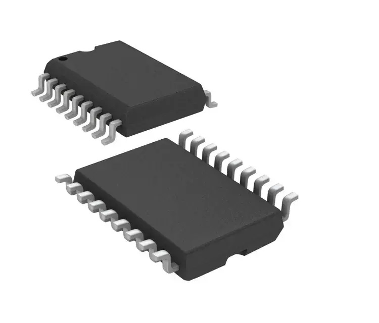
Integrated Circuits
Choosing the Right PCB Material for Your Project
Understanding PCB Material Basics
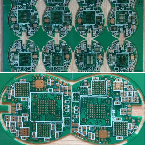
Printed circuit boards are essentially composite structures, consisting of a substrate material and copper layers. The substrate provides mechanical support and electrical insulation, while the copper layers form the conductive pathways that connect different components. The most common substrate materials are various types of epoxy-glass laminates, which offer a balance of cost, performance, and processability. However, other materials, such as polyimide, ceramic, and flexible substrates, are used for specialized applications demanding unique properties.
The choice of substrate material significantly influences the overall characteristics of the PCB. Key properties to consider include the dielectric constant (Dk), dissipation factor (Df), thermal conductivity, and mechanical strength. The dielectric constant, also known as the relative permittivity, describes the ability of the material to store electrical energy. A lower Dk leads to faster signal propagation and reduced signal loss, crucial for high-speed designs. The dissipation factor represents energy loss in the material, impacting signal integrity. High thermal conductivity is important for applications involving high power dissipation, ensuring efficient heat transfer and preventing overheating. Mechanical strength is essential for ensuring the PCB can withstand environmental stress and handling during assembly and operation.
Common PCB Substrate Materials and Their Applications
FR-4 (flame retardant-4) is the most prevalent PCB material due to its low cost, good mechanical properties, and acceptable electrical performance. It's suitable for a wide range of applications, from consumer electronics to industrial control systems. However, its relatively high Dk and Df limit its use in high-frequency applications.
High-frequency applications, such as high-speed digital circuits and microwave systems, often benefit from lower-Dk materials like PTFE (polytetrafluoroethylene), also known as Teflon. PTFE offers excellent electrical performance with low Dk and Df, minimizing signal distortion and improving signal integrity. However, it's significantly more expensive than FR-4 and may have limitations in terms of thermal conductivity and processability.
For applications demanding high thermal conductivity, such as power electronics and LED lighting, aluminum-backed PCBs or materials with embedded copper layers are often preferred. These materials enhance heat dissipation, preventing component failures due to excessive heat. They are typically more expensive than standard FR-4.
Flexible PCBs, using polyimide as the substrate, provide design flexibility and are ideal for applications requiring bending or conforming to irregular shapes. They are commonly found in wearable electronics, medical devices, and automotive applications. However, their mechanical and electrical properties might not always match the performance of rigid PCBs.
Factors Influencing Material Selection
Beyond the inherent properties of the substrate material, several other factors influence the selection process. The operating frequency of the circuit is a key consideration. High-frequency designs often require low-Dk materials to minimize signal loss and distortion. The power dissipation of the components also plays a vital role. High-power applications necessitate materials with excellent thermal conductivity to prevent overheating.
Environmental conditions are another critical factor. The operating temperature range, humidity, and exposure to chemicals or other environmental stresses can impact the longevity and reliability of the PCB. Materials with appropriate temperature ratings and chemical resistance are necessary for harsh environments.
Cost is always a significant consideration. FR-4 offers a good balance of performance and cost-effectiveness, making it suitable for many applications. However, for demanding applications, higher-performance materials may be necessary, even if they are more expensive. The manufacturing process and available fabrication techniques also influence the choice of materials. Some specialized materials might have limited compatibility with standard PCB manufacturing processes.
Conclusion
Choosing the right PCB material is a critical design decision that impacts performance, reliability, and cost. Carefully considering the key properties of various substrate materials, along with the specific requirements of the application, is essential for achieving optimal results. This involves analyzing factors like operating frequency, power dissipation, environmental conditions, and budget constraints. By understanding the trade-offs between different materials, designers can make informed decisions that ensure the success of their projects.

Troubleshooting Common PCB Assembly Issues
Soldering Defects
Solder joints are the very foundation of a PCB's functionality. Defective soldering is a leading cause of assembly failures. Common defects include cold solder joints, which exhibit a dull, grayish appearance and lack a proper metallurgical bond. This often results from insufficient heat, improper solder application, or contamination on the component leads or PCB pads. Identifying and correcting cold solder joints requires careful visual inspection under magnification, potentially aided by X-ray inspection for buried defects. Rework usually involves removing the faulty joint and applying fresh solder with appropriate temperature control.
Another prevalent issue is bridging, where excess solder connects adjacent pads unintentionally. Bridging can be caused by excessive solder paste application, poor stencil design, or insufficient cleaning after the reflow process. The solution often involves careful removal of the excess solder using a wick or a hot air rework station. Prevention involves optimizing solder paste volume, using appropriate stencil apertures, and implementing thorough cleaning procedures.
Finally, tombstoning occurs when one lead of a component stands upright after soldering, resulting from uneven heating or insufficient solder flow. This typically affects surface-mount components with asymmetrically designed leads. Addressing this requires optimizing the reflow profile, ensuring even heat distribution, and possibly choosing components with symmetric leads.
Component Placement Errors
Incorrect component placement is a significant source of PCB assembly problems. Even minor misalignments can lead to shorts, opens, or malfunctioning circuits. This is often attributed to human error during manual placement or inconsistencies in automated placement machines. Careful verification of the bill of materials (BOM) and adherence to precise placement guidelines are essential. Automated optical inspection (AOI) systems can effectively detect component placement errors, enabling early identification and correction.
Another related issue is component orientation errors, where a component is placed upside down or rotated incorrectly. This can lead to functional failures and potentially damage the component or PCB. Clearly marked component footprints and robust quality control procedures, including visual inspection and AOI, are key to preventing this problem. Implementing robust training programs for assembly technicians also significantly reduces human error.
Contamination and Cleaning Issues
Foreign materials on the PCB surface, such as flux residue, fingerprints, or dust particles, can severely impact soldering quality and lead to various assembly defects. Flux residue, if not properly removed, can act as an insulator, preventing proper solder wetting and leading to cold solder joints or opens. Thorough cleaning after the soldering process is therefore essential. Different cleaning methods, such as aqueous cleaning, isopropyl alcohol cleaning, or no-clean flux, are employed depending on the flux type and application requirements.
Contamination can also originate from the manufacturing environment. Dust, hair, or other debris can find their way onto the PCB during assembly, interfering with solderability and potentially leading to shorts. Maintaining a clean and controlled assembly environment, including the use of anti-static mats and appropriate air filtration systems, is critical for preventing contamination-related issues.
Design-Related Issues
While not strictly assembly problems, design flaws can significantly impact the success of the assembly process. Poorly designed PCB layouts, such as cramped component placement or insufficient clearance between traces, can make assembly extremely challenging and prone to errors. Thorough design review and simulation can help identify potential issues before manufacturing begins. Careful consideration of component selection, taking into account their size, shape, and thermal characteristics, is equally important.
Similarly, improper land patterns or trace widths can affect the solderability and reliability of the connections. Adherence to design rules and utilizing appropriate design software with built-in design rule checks (DRC) can mitigate these risks. Collaborative efforts between the design and manufacturing teams are crucial to ensure that the design is both manufacturable and reliable.
Troubleshooting PCB assembly issues requires a systematic approach, combining careful visual inspection, advanced inspection techniques like AOI and X-ray, and a thorough understanding of the assembly process and potential failure mechanisms. Proactive measures, such as meticulous design, robust quality control procedures, and a clean manufacturing environment, significantly reduce the incidence of these problems and contribute to the production of high-quality, reliable electronic products.
Understanding PCB Manufacturing Processes
1. Design and Gerber File Generation
The journey begins with the electronic design, typically created using Electronic Design Automation (EDA) software. This software allows engineers to place components, route traces, and define the overall layout of the PCB. This stage is critical; a poorly designed PCB can lead to signal integrity issues, manufacturing difficulties, and ultimately, product failure. The designer must consider factors such as component placement, trace routing (minimizing signal interference and impedance mismatches), thermal management, and manufacturability. The final design is then exported as a set of Gerber files, which are industry-standard vector files containing all the necessary information for fabrication.
Gerber files are essentially the blueprint for the manufacturer. They define the layers of the PCB, including the copper traces, solder mask, silkscreen, and drill holes. Accurate and complete Gerber files are paramount; any errors can result in costly rework or even complete rejection of the manufactured boards. Manufacturers typically verify the Gerber files before starting production to identify and rectify potential issues upfront. This verification process often involves design rule checks (DRCs) to ensure the design adheres to manufacturing constraints.
2. PCB Fabrication
The actual manufacturing process begins with the creation of the PCB substrate. This substrate typically consists of a base material, such as fiberglass-reinforced epoxy resin (FR4), which provides mechanical strength and electrical insulation. This base material is then clad with thin sheets of copper foil, providing the conductive pathways for the circuitry. The next step involves the photolithographic process, where the copper layers are selectively etched away using photoresist and chemical etchants. This precise etching process leaves behind the desired copper traces defined in the Gerber files.
Multiple layers of copper can be added to create more complex circuit designs. Inner layers are created by laminating copper-clad prepreg (a resin-impregnated fiberglass material) with the copper layers. These layers are then drilled to create vias – holes that connect different layers of the PCB. This process requires extremely high precision to ensure accurate hole placement and size. After drilling, the board undergoes plating to coat the vias and ensure good electrical connectivity between layers. This plating process ensures reliable signal transmission across the different layers of the PCB.
3. Surface Mount Technology (SMT) and Through-Hole Technology (THT)
Once the fabricated PCB is ready, it's time for component placement and soldering. This can involve either Surface Mount Technology (SMT) or Through-Hole Technology (THT), or a combination of both. SMT involves placing surface-mount components directly onto the PCB's surface, while THT involves inserting components with leads that pass through the PCB and are soldered on the opposite side. SMT is more common for modern PCBs due to its higher density and automation capabilities. SMT processes often utilize pick-and-place machines for high-speed, accurate component placement.
After component placement, the PCB undergoes a soldering process, either reflow soldering for SMT components or wave soldering for THT components. Reflow soldering involves heating the PCB to melt the solder paste, which adheres the surface-mount components to the PCB. Wave soldering involves passing the PCB over a wave of molten solder, which joins the leads of THT components. Precise temperature control is crucial in both processes to prevent damage to the components and ensure strong, reliable solder joints.
4. Testing and Quality Control
After assembly, the PCBs undergo rigorous testing to ensure functionality and quality. This testing can involve various methods, including visual inspection, automated optical inspection (AOI), and electrical testing. AOI uses cameras and software to automatically identify defects such as missing components, solder bridges, or shorts. Electrical testing verifies the functionality of the circuit, checking for continuity, shorts, and open circuits. These tests ensure that the finished PCBs meet the required specifications.
Throughout the entire manufacturing process, quality control is paramount. Manufacturers employ various quality control measures at each stage to minimize defects and ensure consistent product quality. This involves regular inspection of materials, processes, and finished products. Statistical process control (SPC) techniques are often used to monitor and improve the manufacturing process. The final stage often involves a functional test to ensure the board operates as intended before packaging and shipping.
Understanding these processes provides a much deeper appreciation for the complexity and precision involved in producing even the simplest PCB. This knowledge is essential for efficient collaboration between designers and manufacturers, ensuring the successful realization of electronic products.
Advanced PCB Design Techniques Explained
Signal Integrity Management
Signal integrity is paramount in high-speed designs. High-frequency signals are susceptible to reflections, crosstalk, and attenuation, leading to signal degradation and malfunction. Advanced techniques focus on minimizing these effects through careful trace routing, impedance control, and the strategic placement of components. Impedance matching ensures efficient signal transmission with minimal reflections, often achieved through controlled trace width and dielectric material selection. This meticulous approach requires specialized simulation tools and a deep understanding of transmission line theory.
Crosstalk, the unwanted coupling of signals between adjacent traces, is mitigated through proper spacing, shielding, and ground plane design. Careful routing and the use of differential signaling can significantly reduce crosstalk. Differential pairs, two traces carrying signals of opposite polarity, are less susceptible to noise and interference compared to single-ended signals. The use of simulation tools like IBIS-AMI models allows designers to predict and mitigate signal integrity issues before prototyping.
Power Integrity and Thermal Management
Efficient power delivery is crucial for reliable operation, particularly in high-power applications. Power integrity management involves minimizing voltage fluctuations and ensuring consistent power supply to all components. This is achieved through meticulous power plane design, including the use of multiple planes and strategically placed decoupling capacitors. Decoupling capacitors act as local reservoirs, supplying instantaneous current demands and preventing voltage drops. Careful consideration of current flow paths is critical to minimize inductance and resistance, ensuring stable power distribution.
Thermal management is equally important, as excessive heat can lead to component failure and reduced lifespan. Advanced techniques involve sophisticated thermal simulations and the strategic placement of heat sinks and vias to dissipate heat effectively. Material selection plays a crucial role, with high thermal conductivity materials like copper often preferred for PCBs in high-power applications. The use of thermal vias, which connect internal layers to external surfaces, improves heat dissipation from internal components.
Advanced Manufacturing Techniques and Design for Manufacturing (DFM)
Modern PCBs are becoming increasingly complex, requiring advanced manufacturing techniques to achieve high precision and reliability. High-density interconnect (HDI) technology allows for a significant increase in component density, leading to smaller and more compact designs. Blind and buried vias, which connect internal layers without extending to the top or bottom surface, enhance circuit complexity and reduce board height. Understanding the capabilities and limitations of these techniques is essential for successful PCB design.
Design for Manufacturing (DFM) is a critical aspect of advanced PCB design. DFM involves considering the manufacturing process early in the design phase to ensure manufacturability and minimize costs. This includes adhering to manufacturing tolerances, choosing appropriate materials and finishes, and designing for automated assembly processes. Collaboration with manufacturers is crucial for successful DFM implementation.
High-Speed Design Considerations
Designing for high-speed applications necessitates a different approach compared to lower-speed designs. Signal integrity, as mentioned earlier, is paramount. However, the challenges extend beyond simple impedance control. Considerations such as return path inductance, differential pair skew, and electromagnetic interference (EMI) become increasingly important. Careful control of trace lengths, the use of controlled impedance structures, and proper grounding techniques are essential to mitigate these effects.
Simulation and analysis are crucial components of high-speed design. Sophisticated electromagnetic simulation tools are used to predict signal integrity and EMI issues. These tools allow designers to identify and address potential problems before physical prototyping, saving time and resources. The iterative process of simulation, analysis, and design refinement is crucial for achieving optimal performance in high-speed designs.
In conclusion, mastering advanced PCB design techniques requires a multidisciplinary approach, combining theoretical understanding with practical experience and the utilization of advanced simulation tools. By embracing these techniques, designers can create more robust, efficient, and reliable electronic products capable of meeting the ever-increasing demands of the modern world.REPORT

